Q.01 A material which has a resistance in between that an insulators and of a conductor is known as___
A. semiconductor materials
B. insulations
C. conductors
D. power electronics
Ans.: A
Q.02 which of the main features of intrinsic semiconductors?
A. it has negative temperature coefficient
B. its resistance is more than conductors and less then insulators
C. ±4 valance electrons
D. all of the above
Ans.: D
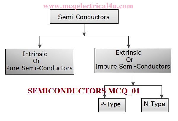
Q.03 A semi conductors is in its purest form is known as___.
A. extrinsic semi conductors
B. intrinsic semiconductors
C. combinations of A and B
D. trivalent substance
Ans.: B
Q.04 The conductivity of semiconductor is to be increased by adding impurity elements is known as___
A. doping
B. increase energy gap
C. reduced energy gap
D. increase forbidden gap
Ans.: A
Q.05 When the number of free electrons increased the doped semiconductor is ____
A. negative or N-type
B. positive or P-type
C. negative or P-type
D. positive or N-type
Ans.: A
Q.06 Which of the following is/are true?
A. for metal resistivity 10-8 ohm-m
B. for insulator resistivity 1012 to 1020 ohm-m
C. for semiconductor resistivity 10-4 to 107 ohm-m
D. all of the above
Ans.: D
Q.07 In semiconductor the highest filled band is called___
A. valance band
B. conduction band
C. forbidden gap
D. none of the above
Ans.: A
Q.08 The conduction band and valance band are separated by region is called
A. valance band
B. conduction band
C. forbidden energy gap
D. none of the above
Ans.: C
Q.09 The energy bands which is completely filled at zero K is known as____
A. conduction band
B. valance band
C. energy band
D. forbidden energy band
Ans.: B
Q.10 Which of the following band has highest energy level?
A. conduction band
B. valance band
C. energy band
D. forbidden energy band
Ans.: A
Q.11 At absolute zero temperature, semiconductors behaves as___
A. perfect conductor
B. perfect insulators
C. extrinsic semiconductor
D. none of the above
Ans.: B
Q.12 The forbidden energy gap of silicon is ____and for germanium is ____
A. 1.1 eV; 1.1 eV
B. 0.72 eV; 1.1 eV
C. 1.1 eV; 0.72 eV
D. 0.72 eV; 0.72 eV
Ans.: C
Q.13 In semiconductor the forbidden energy gap between the conduction band and valence band is ____
A. about 5 eV
B. 1 eV
C. 2.5 eV
D. 7.2 eV
Ans.: B
Q.14 In semiconductor the vacant energy state in the valance band is known as__
A. holes
B. positive charge
C. electrons
D. negative charges
Ans.: A
Q.15 Holes in semiconductor drifts in ____ to electrons with ___ speed.
A. same direction; lesser
B. opposite direction; lesser
C. same direction; more
D. opposite direction; more
Ans.: B